
Research
Our research explores energy systems and technologies—and the science behind them—for a future powered by affordable, abundant, and reliable energy.
This research supports NREL's vision of an affordable and secure energy future.
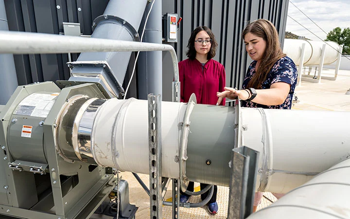
Research Facilities
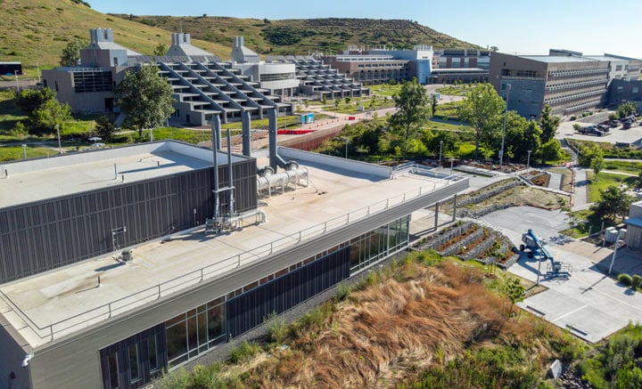
Learn about NREL's state-of-the-art facilities and the research conducted within our laboratories.
Share
Last Updated July 24, 2025